~written by Jeff Duncan, Dataram Memory Blog Team Member
In 40 years, memories have gone from less than 1K bytes capacity, a size of 15” x 15” x 1”, 2 microsecond speeds (0.000002 seconds) using core memory and no standards, to 32 Gbytes, a size of 5.3” x 1.19 x .3”, 13.75 nanosecond speeds (.00000001375 second) using semiconductor memory and now using industry standard designs.
In the late 60s, main memory was composed of core memory. These modules were all custom designs, all shapes and physical sizes for each computer OEM. The base component in core memory was 20 mil ferrite cores. These needed three to four wires to be strung through the center of each core. X and Y axis wires for selection of the core to be accessed (a bit) in a given array, a third to sense change and inhibit change (sense/inhibit line) to prevent a core from switching. In earlier core memory’s 4 lines were used sense and inhibit were separate wires and the cores were bigger. A good basic “how do core memories work” can be found at http://en.wikipedia.org/wiki/Magnetic-core_memory or on many other sites.
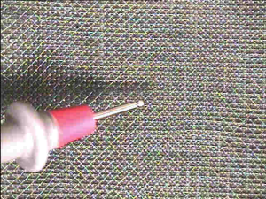
When I got involved in the mid-1970s, we were using 18-mil (0.018 inch) cores with three 3-mil (0.003 inch) wires. The first photo below is of the cores next to a pencil point. Looks like a fly left something behind. To give you a sense of size, the next photo shows an electronic test probe (as small as a pencil point) against a core memory array.
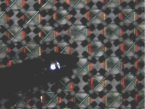
Under additional magnification, the previous test probe and cores:
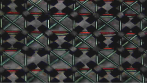
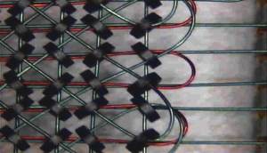
By the way, people manually strung the wires through the core fields viewing through a microscope. This was very labor-intensive and tedious work that could take weeks, depending on the array (memory) size. The photos that follow are the previous array photos magnified more. So, core memory took a long time to manufacture, was big and heavy, and was fairly expensive.
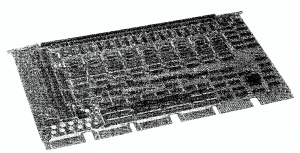
The core array was attached to a Printed Circuit Board for stability, and that core stack assembly was sometimes soldered to an electronics board or attached via connector system. In the following photo, a Dataram Corp compatible DEC (Digital Equipment Corp) PDP-11 series Unibus core memory module (32Kbytes) has the core stack assembly underneath the controlling electronics board attached through connectors. Unlike most of today’s memory modules besides the analog devices (discrete transistors, diodes, transformers, resistors) used to drive the core array, there were many semiconductor SSI (Small Scale Integration) logic devices to interface to the memory bus. This made these designs much more complex.
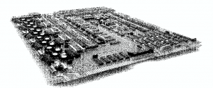
The next photo of a core memory module was our custom design used as a generic module (32Kbytes). We would install multiple units in a chassis and they would be interface to a computer bus. Typically, they were used for main memory, extended memory and the first Solid States Disks.
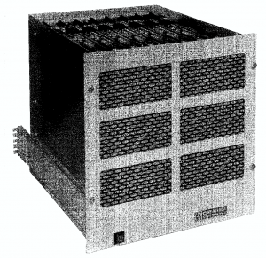
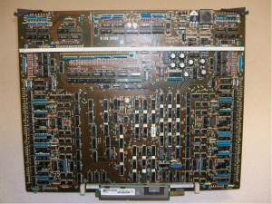
In the late 1970s we built a state-of-the-art 256Kbytes module which we used for extended memory and solid state disk emulations for DEC, Data General, Honeywell, Perkin Elmer, Interdata, Varian, etc. The memory system was 128K x 18 (256Kbytes) and was 16.5 inches by 13.5 inches by 1.75 inches. They would be installed in the chassis in the following photo with an interface for a specific computer type and disk emulation. This would provide a whopping 2Mbytes of storage in a 19-inch rack mount chassis.
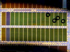
Then in the mid 1980s we started using semiconductor memory made from silicon – more specifically, DRAM (Dynamic Random Access Memory). This was very, very small, and much faster than core memory. The following photo gives you a sense of size. Four 18-mil cores are sitting on a DRAM die in wafer form. You are looking at millions of bits of semiconductor memory vs. four bits of core memory.
We probably converted over to DRAM memory in the 4Kbit days. Although we were using semiconductor memory, the computer OEM still used the large board sizes and similar bus interfaces, thus the control and buffer logic was still I every memory board.
As time went on, semiconductor cells were getting so small someone finally came up with the idea of putting the memory controller (all the logic) on the CPU board and the memory boards would just have DRAM on them. The SIMM came about (Single In-line Memory Module). These modules would plug right into connectors on the CPU board. SIMMs were typically 1Mx8/9 modules, so for most computers you needed two modules for 16 bit systems plus two bits for parity. The finger edge connectors on these boards were electrically connected top and bottom (Single In-line). Next was the dual in-line module (DIMM), which simply meant the top and bottom side connector fingers were independent allowing for more pin-outs for longer bit widths.
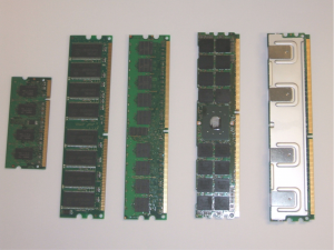
In the meantime DRAM Manufacturers and JEDEC (Joint Electron Devices Engineering Council) established standards for DRAM/Module pin-out, DRAM/Module packages sizes, DRAM/Module specs, etc. DRAM capacities increased 1Mx1, 4Mx1, 1Mx4, 16Mx1, 4Mx4 and on and on until today we are using 4Gbit technology DDR3 (1Gx4, 512Mx8, 256Mx16, 128Mx32). Memory interfaces have gone from FPM (Fast Page Mode), EDO (Extended Data Out), SDRAM, (Synchronous DRAM), DDR1 (Double Data Rate 1 SDRAM), DDR2 (Double Data Rate 2 SDRAM), DDR3(Double Data Rate 3 SDRAM) and heading to the mainstream are DDR4 (Double Data Rate 4 SDRAM). All these interfaces were necessary to handle speed increases. Also multiple standard modules such as SODIMM, MICRO-DIMM, MINI-DIMM, VLP DIMM, RDIMM, FBDIMM, etc., have been used. The next photo has examples of these modules, plus there are websites that define all these configurations. DRAM package sizes and mounting styles also have changed as more pin-outs and faster speeds became available such as SOJ (Small Outline J lead), TSOP(Tiny Small Outline Package) and now BGA (Ball Grid Array).
So to recap, from a 256Kbyte core memory that was 16.5 inches by 13.5 inches by 1.75 inches to a 32Gbyte LRDIMM (Load Reduced DIMM) that is 5.3 inches by 1.2 inches by 0.29 inches –pretty amazing. An example of these two memories are in the following photo. The 32Gbyte module is at the bottom of the photo leaning against the 256Kbyte module. It would take 131,072 of the 256Kbyte modules to equal one of the 32 Gbyte modules at the bottom of the photo.


